Categories
Test Adapters UNIMET
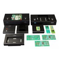
Test adapters (TAxx) further extend the capability of base test station (M3000, UNIMET 3000, UNIMET 2020). They contain additional instruments necessary to test dedicated family of devices. We've successfully followed up on the development of M3000 test adapters originaly designed by SZ Testsysteme GmbH in Amerang. Our newly designed Test adapters are TA37 (Discrete semiconductors) and TA39 (OpAmps) meet new demands of modern semicondcutor era. We can of course still offer slightly redesigned, yet still compatible, versions of original Test Adapters by SZ Testsyteme. All TAs are controlled by SCADUS, our universal test software.
A complete delivered package of TAxx contains also so called GOLDEN devices i. e. devices with protocolled test results and reference Socket Adapters with dedicated device socket and application circuitry.
RLC | Monostable relays, Bistable relays with 1 or 2 coils | Regulators | Optocouplers with analog I/O, 1–4 devices in package | Bipolar Transistors (NPN, PNP, Low power, Darlington, Field effect transistors (N-channel, P-channel, Power-MOS), Diodes, Zenner diodes, Arrays, 2000V optional | A/D Converters, D/A Converters, Sample & Hold devices, Voltage references | Operational amplifiers , Comparators, Chopper OA | CMOS, HCMOS, NMOS , PMOS , TTL (LS, ALS, S, FAST, etc.), DTL, HTL, ECL | Low side switches, High side switches | Static RAM, ROM, PROM, EPROM, EEPROM | Processors and peripheries, Memories, Logic arrays, TTL logic devices | Bipolar transistors (NPN, PNP, Low power, Darlington), Field effect transistors (N-channel, P-channel, Power-MOS), Diodes, Zener diodes, Arrays, 2 000 V optional | Avalance energy
TA37
Testing: Transistors (NPN, PNP, Low power, Darlington, Field effect transistors (N-channel, P-channel, Power-MOS)), Diodes, Zenner diodes, Arrays, 2000V optional.
Testing ranges: 600V/100A
Parameters - Bipolar Transistors
- Breakdown voltage VCE0(BR)
- Breakdown voltage VCES(BR)
- Saturation voltage VCE(sat)
- Saturation voltage VCB0
- Breakdown voltage VCB0
- Breakdown voltage VEB0
- Diode forward voltage VF(diode)
- Collector/Emitter cutoff current ICEO, ICBO, IEBO
- On voltage VBE(on)
- DC current gain hfe(DC)
- AC current gain h21e(AC)
Parameters – Triacs & Thyristors
- Gate trigger current IGT
- Gate trigger voltage VGT
- Off-state leakage current IDO
- Hold current IH
- Latch current IL
Parameters – Diodes & Zenner Diodes
- Forward voltage VF
- Reverse voltage VR
- Zenner voltage VZ
- Reverse leakage current IR
- Dynamic resistance DC RDdyn
- Dynamic resistance AC Rz
Parameters – MOS-FETs
- Breakdown voltage V(BR)DSS
- Thermal resistance Rth
- Inverse diode voltage VSD
- Gate threshold voltage VGS
- On resistance RDS(on)
- Forward transconductance gfs
- Forward/Reverse leakage current IGSS
- On voltage VDS(on)
- On-state drain current ID(on)
TA39
Testing: Operational amplifiers, Comparators, Chopper OA.
- Input offset voltage VOS
- Offset voltage adjustment range
- Positive / negative supply current VRGOS
- Input bias current IB
- Input bias current IB+/IB
- Input offset current IOS
- Large signal voltage gain AVO
- Slew rate ±SR+/SR
- Common mode rejection ratio CMRR
- Power supply rejection ratio PSRR+/PSRR
- Output voltage swing VO+/VO
- Gain bandwidth product GBP
- Forward transductance GM
- Short circuit current ISC
- Function test FCT
TA01
RLC Test Adapter.
Testing:
- Resistors
- Capacitors
- Inductors
You can measure resistance, capacitance and inductance. You also can set up a reference value and compare in percent points the deviation from reference value. For capacitors and inductors adapter measures also tangens delta – 1/Q value.
TA02B
Testing: Monostable relays, Bistable relays with 1 or 2 coils.
Testable parameters:
- Coil resistance RCOIL
- Diode forward voltage Vtwd
- Case test ICASE
- Contact resistance RCONTACT
- Leakage current Ileak
- Function test FCT
- Pickup energization Voperate, Ioperate
- Dropout energization Vrelease, Irelease
- Operate time toperate, (V), (I)
- Release time trelease, (V), (I)
- Transit time ttransit, (V), (I)
- Synchronicity tsync
- Bounce time tbounce
- Bounce number nbounce
TA03B
Testing: Regulators
- Output voltage Vo
- Line regulation RegLine
- Load regulation RegLoad
- Quiescent current Iq
- Ripple rejection SVR
- Reset leakage current Ileak
- Short circuit current Isc
- Dropout voltage DOV
- Reset delay time Tres
- Reset pulse width Trpw
- Reset output voltage Vres
TA06B
Testing: Optocouplers with analog I/O, 1–4 devices in package.
- Current Transfer Ratio CTR
- Saturation Voltage or Output Voltage Vsat, Vout
- Dark Current or Output Current IOH, IOUT
- Diode Forward Voltage or Input Voltage Vfd, Vin
- Diode Breakdown Voltage Vbr
- Switch-on Time ton
- Switch-off Time toff
- Reverse Current or Input Current Iin
- Supply Current ICC
- Output Short Current IOS
- Enable Current IE
- Threshold or Hysteresis Currents/Voltages I/UTH
TA08B
Testing: A/D Converters, D/A Converters, Sample & Hold devices, Voltage references.
TA10B
Testing: CMOS, HCMOS, NMOS, PMOS, TTL (LS, ALS, S, FAST, etc.), DTL, HTL, ECL.
TA15B
Testing: Low side switches, High side switches.
- 6 programmable reference sources
- Power source 45V/100A (peak)
- Pin driver ±12V
- Differential amplifier
- Expansion VI-Source PSM51 ±51V/5A
TA16B
Testing: Static RAM, ROM, PROM, EPROM, EEPROM.
- Addres bits 0…16
- Data bits 0…16
- Control bits 0…7
- Access time 0…630ms
- Programmable sources voltage/current, counters and the others instruments
TA17B
Testing: Processors and peripheries, Memories, Logic arrays, TTL logic devices.
Test Groups Architecture
- 48 bidirectional test signals
- Data rate up to 10 MHz
- Hardware test evaluating in the input mode
- Expected data stored in the output channel
- Input data compared with the expected data
- Fail marks of the input vectors stored
- 10-bit fail events counter
Parameters
- Parameter - Group 0 - Groups 1 .. 5
- Signals Number
- 8 bidirectional
- Pattern Out Depth
- 2048 (Standard)
- 32768 (max)
- Pattern In Depth
- 2048 (Standard)
- 32768 (max)
- Direction Control
- single (In or Out)
- common (In or Out)
- single (In or Out)
- Output Timing
- single (Start/Stop)
- common (Start/Stop)
- single (Start/Stop)
- Input Timing common (Load Point)
- Format Control common
- Output Format *
- return-to-zero
- return-to-one
- surround-by-complement
- non-return
- Input Format
- data
- data
- fail marks
- fail number (0..65535)
- data
- FIFO Unit Control
- Reset and Retransmit
- FIFO Unit Flags
- Empty and Full
- Synchronization
- independent In and Out
- Output Low Level
- 0.3 V .. 5.5 V
- Output High Level
- 0.3 V .. 5.5 V
- Input Threshold
- 0.3 V .. 5.5 V
- Timing Range
- 255 ns or 1275 ns
„*“ for all pins in the group


